Surface technology and surface characterization with regard to forming technologies are the focus of the PtU’s work. In order to facilitate research activity in this field, the PtU purchased a Scanning Electron Microscope (SEM) in 2010. Due to the significantly shorter wavelength of an electron beam, microscopic analysis can be acquired at much higher magnifications than with regular light microscopes.
The three acquisition modes secondary electron, backscattering compo and backscattering topo enable the plastic illustration of material contrasts and topographies at various intensities. The analysis of nonconductive materials like paper or compound-materials are also possible due to the low vacuum mode.
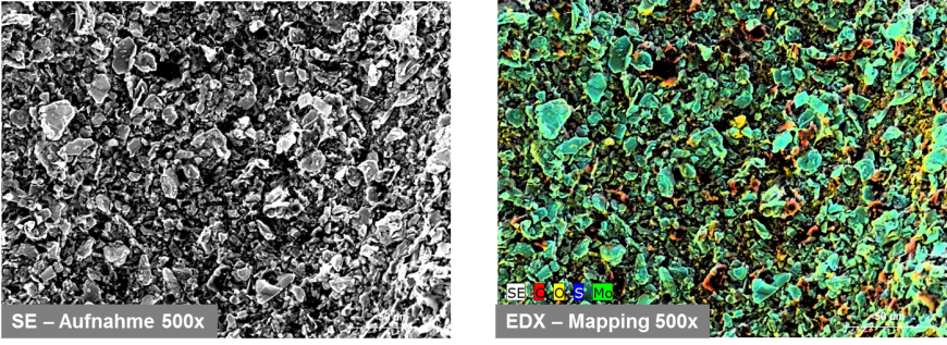
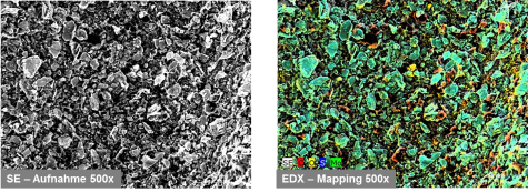
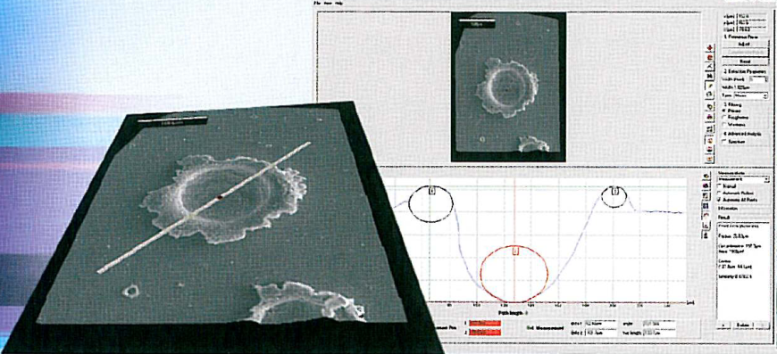
In addition to the purely microscopic imaging of the samples' surface, the elementary composition of the specimen can be analyzed. During the interaction of the electron beam with the surface, energetic specific X-ray-radiation is emitted. Due to that, the elementary composition of the samples’ material surface structures can be gathered by energy-dispersive X-ray spectroscopy (EDX). Furthermore, the surface topography can also be analyzed three dimensionally. Due to a digital compilation of two dimensional surface images by a computer program, the topography can be evaluated three dimensionally.

Technical data
- magnification: 5x – 300,000x
- resolution (SE): 3 nm (30 kV)
- resolution (LV): 4 nm (30 kV)
- traverse paths:
x = 120 mm
y = 100 mm
z = 80 mm
t = -10° – 90°
r = 360° endless